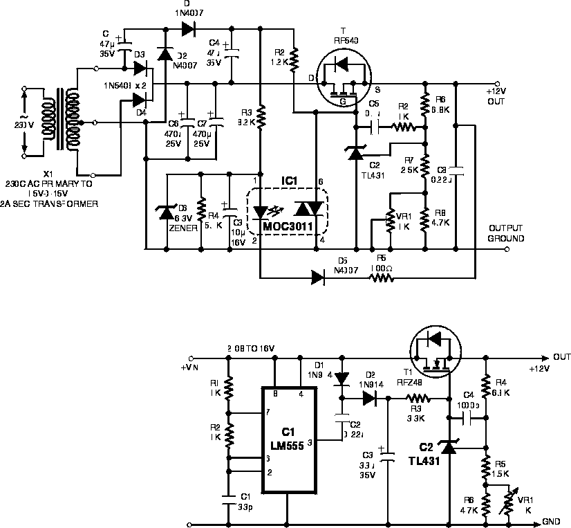
Electronic circuits > Power Supplies > Ultra low drop linear voltage regulator
Ultra low drop linear voltage regulator The circuit is a MOSFET based linear voltage regulator with a voltage drop
of as low as 60 mV at 1 ampere. Drop of a fewer millivolts is possible with
better MOSFETs having lower RDS(on) resistance. The circuit in Fig. 1 uses
15V-0-15V secondary from a step-down transformer and employs an n-channel MOSFET
IRF 540 to get the regulated 12V output from DC input, which could be as low as
12.06V. The gate drive voltage required for the MOSFET is generated using a
voltage doubler circuit consisting of diodes D1 and D2 and capacitors C1 and C4.
To turn the MOSFET fully on, the gate terminal should be around 10V above the
source terminal which is connected to the output here. The voltage doubler feeds
this voltage to the gate through resistor R1. Adjustable shunt regulator TL431
(IC2) is used here as an error amplifier, and it dynamically adjusts the gate
voltage to maintain the regulation at the output. With adequate heatsink for the
MOSFET, the circuit can provide up to 3A output at slightly elevated minimum
voltage drop. Trimpot VR1 in the circuit is used for fine adjustment of the
output voltage. Combination of capacitor C5 and resistor R2 provides
error-amplifier compensation. The circuit is provided with a short-circuit
crow-bar protection to guard the components against over-stress during
accidental short at the output. This crow-bar protection will work as follows:
Under normal working conditions, the voltage across capacitor C3 will be 6.3V
and diode D5 will be in the off state since it will be reverse-biased with the
output voltage of 12V. However, during output short-circuit condition, the
output will momentarily drop, causing D5 to conduct and the opto-triac MOC3011
(IC1) will get triggered, pulling down the gate voltage to ground, and thus
limiting the output current. The circuit will remain latched in this state, and
input voltage has to be switched off to reset the circuit. The circuit shown in
Fig. 2 follows a similar scheme. It can be utilised when the regulator has to
work from a DC rail in place of 15V-0-15V AC supply. The gate voltage here is
generated using an LM555 charge pump circuit as follows: When 555 output is low,
capacitor C2 will get charged through diode D1 to the input voltage. In the next
half cycle, when the 555 output goes high, capacitor C3 will get charged to
almost double the input voltage. The rest of the circuit works in a similar
fashion as the circuit of Fig. 1. These circuits above will help reduce
power-loss by allowing to keep lower input voltage range to the regulator during
initial design or even in existing circuits. This will keep the output regulated
with relatively low input voltage compared to the conventional regulators. The
minimum voltage drop can be further reduced using low RDS(on) MOSFETs or by
paralleling them

Published on: 2004-08-21 (3642 reads)
[ Back | Home ] |